|
for Anim. Click BACK to return here.
|
|
|
|
Inverting Op Amp
|
Non-Inverting Op Amp
|
|
|
..
|
-
|
An
Amplifier is made of:
1)
A Gain "Block" (ideally possessing infinite
gain)
2)
Feedback
3)
A Network that sets the amount of feedback (e.g.,
resistors)
|
--
|
|
--
|
If
the above Carved-in-Stone
requirements are met, the characteristics of the
Amplifier are determined by the feedback network only,
not the gain block, nor the transistors used in the
gain block's construction. That is, the more "raw"
gain that is available to the amplifier, the less
effect components have on fidelity.
Saying
it another way:
Feedback
combined with >>Gain, reduces
Distortion--improves Fidelity!
Of course, the
world is not made that way; there are no Ideal
Amplifiers, no infinite gain Gain Blocks; so the name
of the game is to do the best you can--up to the point
of satisfying the Amplifier design requirements.
|
|
|
Think
of feedback as a continuous comparison between the
input signal and what the amplifier is putting out. As
this comparison is made, ERRORS between the real
signal and any lack of faithfulness of the amplifier
output tend to be corrected.
These corrections
are made as a result of the feedback and the LARGE
open loop GAIN of the opamp.
|
|
|
Example:
If you need an amplifier with
a gain of, say 10, and you have a gain block (op amp)
possessing gain in the neighborhood of >200 K (open
loop), you use a feedback network that allows signal
cancellation such that all but enough to allow the
output to be ten times greater than the input. This
results in a very stable and low distortion amplifier
with a gain of 10.
|
|
|
The absolute gain of an
amplifier is a function of the feedback network
precision, not the open loop gain of the op amp
(within limits). This statement is more true, the
greater the open-loop gain of the op amp device.
|
|
|
|
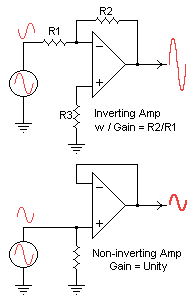
Single
Ended Inverting Amp
|
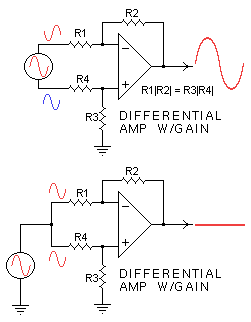
Differential
Mode = Acceptance
|
|
|
|
|
Single
Ended Noninverting Amp
|
Common
Mode = Rejection (CMR)
|
|
|
..
|
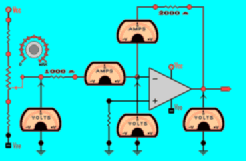
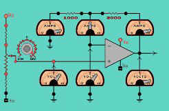
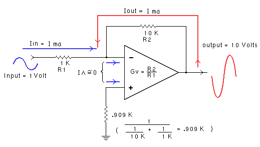
Anyway, because of the aforementioned (I've always
wanted to use that word in a sentence), let's say a
current of 1 milliamp is caused to flow to the
inverting input pin through the 1000 ohm input
resistor, R1, the Op Amp tries to maintain
equilibrium, i.e., no current flow in that input pin.
To do this marvelous feat, it generates an output
voltage of the opposite polarity, which maintains that
1 milliamp to flow through the 10 K feedback resistor,
R2 to the output. Because the feedback resistor is ten
times the value of the input resistor, it will require
ten times the voltage to cause that same 1 ma to flow.
The view from the input pin: there is a current of 1
milliamp coming down the input resistor, and at the
same time, there is a current of 1 milliamp coming
from the feedback resistor. there is no current left
over for the input pin; therefore satisfying the zero
current requirement of the Op Amp. "Eureka!"
you have a signal ten times larger, than you started
with, and boys and girls, there's not a mirror in
sight!
|
|
|
|
OK. OK. If you're so
smart: what the Hell is Virtual Ground ?
Explain that if you can! I just did! Because no matter
(within reason) how much current was made to flow in
the input resistor, no voltage change was seen at the
other end--the input pin. If the resistor had been
attached to ground, the effect would have been the
same: current flow into the resistor; no voltage at
the other end. I know it sounds silly, but hang on for
one more point. Let us say you use a CMOS Op Amp
having an input impedance of tens of thousands of
megohms--with the same resistor values as the example
above. You apply a signal generator that has a output
impedance of 1000 ohms. We know that if we apply that
generator to a 1000 ohm load, the output voltage of
the generator will drop by 6dB (50%). Now apply this
generator to our CMOS Op Amp and measure the generator
output level before and after: the output will be down
by--you guessed it--6dB. In fact, nothing has changed,
whether its a CMOS or a BJT Op Amp, the principle is
the same: if the Op Amp has enough gain, the device
itself has no discernible effect on the circuit.
Now! The non-inverting input
is another story altogether! Its input impedance is
affected by the device type. In the CMOS case the
non-inverting input pin--as mentioned earlier--has the
impedances approaching tens of thousands of megohms.
This high impedance input can be used to great
advantage: in sample & hold circuits, peak
detectors--you name it.
|
|
|
|
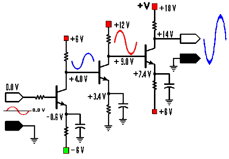
If you've ever designed a DC
(direct coupled) amplifier with more than two
stages, you've discovered the stair-step
phenomenon: as each collector is connected to the base
of the succeeding stage, the higher the emitter/base
bias or offset must be.
|
|
|
|
Multiple
stage "stair-stepping" DC (direct coupled)
Amplifier
|
|
|
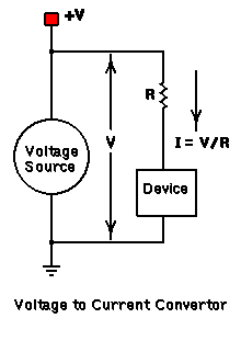
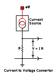
A
resistor is a voltage to current
converter. A resistor is also a current to
voltage converter. How does it know which it is at the
time?
|
|
|
|
A
resistor is a voltage to current converter.
|
A
resistor is a current to voltage converter.
|
|
|
Operational
Amplifiers
The "Op Amp" is one of
the most valuable and versatile integrated circuits to
ever come down-the-pike. If you want to spend a Month
-of-Sundays abusing yourself, and you've run out of
sharp sticks: build an Op Amp, from scratch--one that
works as well as the monolithic version; or for that
matter, one that works period! There is almost no
circuit design that can't benefit from the use of the
Op Amp.
From the 741--the
first internally compensated Op Amp, and son of the
709--to the super-fast near GHz Op Amps; these little
"boogers" are easy to use: If you bypass,
decouple, and use common sense... Ha! There I
said it. Ha!
"How does this Damn thing work?" "Very
well thank you."
Lets keep this simple:
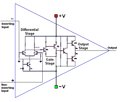
The Op Amp is basically three amplifiers or stages.
The input differential stage; the gain stage, and the
output stage.
|
|
Input
Stage
|
Gain
Stage
|
Output
Stage
|
|
|
|
|
|
|
Op-Amp-Stages
|
|
|
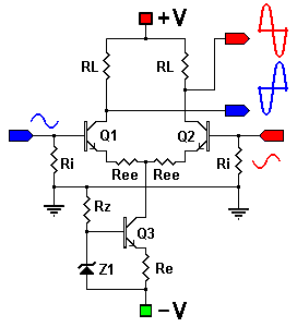
The differential
stage is the heart of the Op Amp, and the
most confusing. If you think of the Op Amp as a
differential amplifier --because that's what it
is--and think of the other stages as parts of the
same, then the confusion may drop about 20dB, or go up
thirty.
|
|
|
|
|
Showing
Differential Mode Input
|
Showing Common
Mode Input
|
|
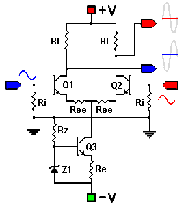
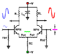
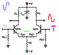
The Op Amp is a current device in, and a
voltage device out. The Op Amp's output is not
dependent on the amplitude of the input current per
se, but on the current difference between the input
pins. If you tied both pins together and applied a
very large signal to this connection: the output would
be unchanged, or at most, a weak crappy replica of the
input. This is known as common
mode rejection, (CMR).
|
|
|
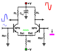
Input Stage
|
|
|
|
|
|
Differential
Input Stage
Demonstrating
Offset
|
|
|
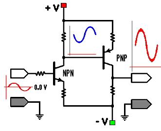
Of course that's why GOD made PNP
transistors (we finally know the reason), but this can
be taxing and not always satisfactory.
|
|
The
reason GOD made PNP transistors
|
|
|
|
Gain Stage
|
|
Enter the Op Amp: it has the facility of
not having--by nature--any offset between input and
output. You could DC couple zillions of OP Amps in
cascade. When configured as an inverting amplifier
with some gain (Gv), its sole aim in life is to not
allow any current to flow in the inverting pin. And,
because it has in its arsenal, gains on the order of
several hundreds of thousands (100k to 600k), it has
no problem in doing just that: No Current In!
Remember: it is a current input, and a voltage output
device.
|
|
|
|
|
|
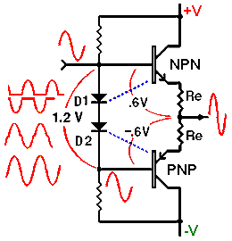
Output
Buffer Stage
|
Another
Output Buffer Stage
|
|
|
|
|
|
|
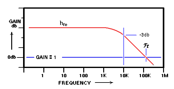
Gain Bandwidth
Product
|
|
|
|
|
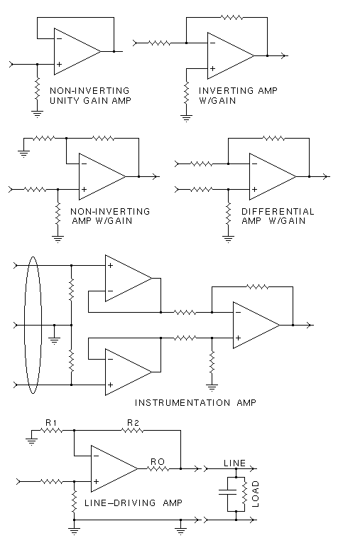
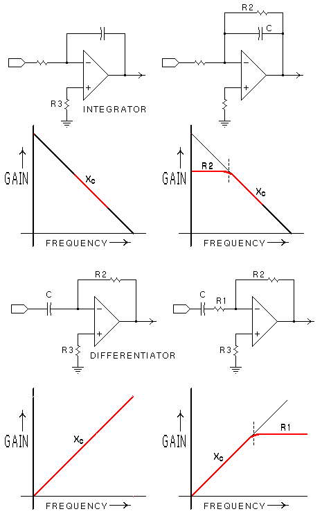
Misc Op Amp Circuits
|
|
|
|
|
|
|
|
|
|
|
|
|
|