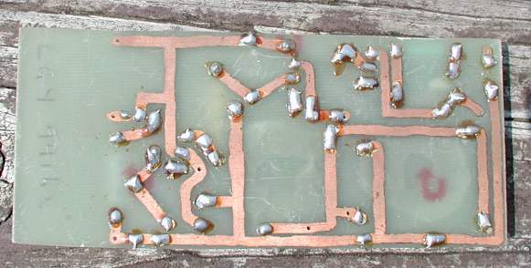
This was crude but effective at the time
Updated May 26, 2014
One way of making high quality prototype printed circuit boards is using a negative film. When exposing the film on a contact frame with sensitized copper clad boards that have been coated with KPR® photo resist or laminated photo resist film, the light hardens the resist where the film is transparent. When the board is developed, the areas of the board that weren't exposed to light melts away. The resist "resists" the copper etching solution leaving behind the copper printed circuit.
Kodalith® Ortho Type 3 is/was the industry standard film used in this process. It was a very high contrast film and gave excellent results. Exposing time is somewhat critical but developing times, stop, and fixer time is not critical.
A bit of history: Way back in the early 1960's, as a child I was impressed with the concept of printed circuits. The first place I saw them was in the first portable transistor radios from Japan. I remember carefully cutting aluminum foil, gluing it on a board and trying to solder parts to the foil. After many attempts I gave up and found other things to occupy myself. Years later the concept of resist pens allowed me to paint the resist on copper boards as shown below.
This was crude but effective at the time
Once the resist dried, the board was etched with ferric chloride. It did well for prototypes and small one-of-a-kind projects.
In the mid 1970's I had a job laying out "artwork" using Bishop Graphics pads and lines on gridded acetate or Mylar film on a light table. By 1974 I was designing a few boards a week for the company I was employed. Once the layout was complete we sent the "artwork" to a local printing business where they would place the film on a huge floor camera or vertical camera. We'd lay the board out at 200% the original size. This would give us a very sharp and clean film when reduced to 50% the original size, reduced any pinholes in the emulsion of the film, and halved any slight errors in registration.
The film was used by the circuitboard prototyping company to make the first test boards. Once the design was verified, the films were sent on to the fabrication house to make the production run of boards.
This has been the norm for many years to come. Even as late as 2010 I was able to take my artwork to a local printer and pick up a negative film sometimes the same day for about $10 for an 8" X 10" film.
In just a few short years just about all printing businesses, even the local small town printers have gone from using film to burn plates for offset printing to a "direct-to-plate" method thereby eliminating the whole film process.
This all came as a surprise to me when I went all around our town looking for someone with a vertical camera and film processing system.
Most print shops just disposed of their cameras and film supplies at the junk yard. Occasionally you will see some of these huge cameras (the size of a refrigerator) or a film processor/printer on eBay.
If you need just a few pieces of film and are looking for someone to make them I may be setting up a service with one day turn-around. See the end of this page for details.
If you're really serious about making lots of prototypes and want to make your own film you will need chemicals, trays, tongs, red safety light, storage bottles, timers, etc. besides a monster vertical camera. You can also look for a copy stand. I have one in storage. It will reduce and make films too. You can find chemicals and equipment on eBay and some suppliers like http://www/freestylephoto.biz and http://www.bhphotovideo.com .
Chemicals such as Kodalith Ortho film developer may be new old stock but I have found them still usable after 20 years if stored properly. I happened to find some jars of Kodalith developer A and B some 40 years old that still work. You will also need Fixer. This shouldn't go bad for a long time if the powder is stored in a tightly sealed jar. A stop bath is optional but not really necessary. Plain water does fine. Used Kodalith developer has a short life span. When part A and B are mixed you may have only a day or so to use. I have been told Dektol paper developer will work too. I haven't tried it but will report back here with my results. Used fixer will last much longer. Months if used sparingly. I only mix enough developer and fixer to do small jobs so as not to waste it. Both Freestyle and B&H still sell chemicals and film but who knows for how long?
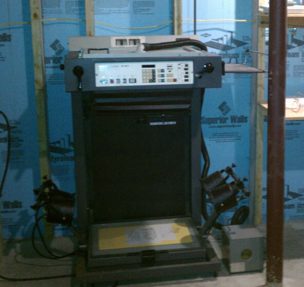
Finding a floor camera might be a good bit harder. I was fortunate that the local newspaper was wanting to dispose of their camera since they went all digital. They were going to take it to the junk yard but the camera operator there knew me and asked if I wanted it. I just had to haul it away. What a find! Note the vacuum pump on the lower right side.
If you are serious about making negatives in large quantities or wanting to make money providing this service it might be a good investment. You just need to find a small print shop in a town near you that's willing to dump their unit. You might be the recipient of a lot of free chemicals and film too.
Since I am always in need of some quick boards I need to make the films myself so I can make the prototype boards. It is not unusual for me to design a circuit, lay it out in the morning, print it, convert to film, expose the board, etch and drill the board before lunch, stuff it with parts and have the circuit functioning before 2 PM the same day. I recently set up my camera and started scrounging film and chemicals. So far the links shown above are companies have what I need.
More recently there is an iron on process from http://www.pcbfx.com that eliminates much of this process. It is a one-shot deal. Meant for making single boards only. Personally I'm not quite satisfied with quality and consistency but you may have better results.
I happen to have some old chemical powders more than 35 years old! I mixed the chemicals to what I feel were the proper portions and tried a negative. It worked first time! I made my first negative film and it came out perfect.
The following instructions and procedures are for making successful films.
I use a computer program to lay out boards now. There are some free versions and then there are very expensive versions. A free one is called EagleCad from http://www.cadsoftusa.com . I haven't used it though. I used Tango for many years but it was primarily an expensive DOS version. The Windows version is very expensive too and I think obsolete now. A very popular and upcoming PC CAD software program is Sprint Layout 6.0 from http://www.abacom-online.de/uk/html/sprint-layout.html It costs about US$60 and downloadable from Germany and it has many professional features.
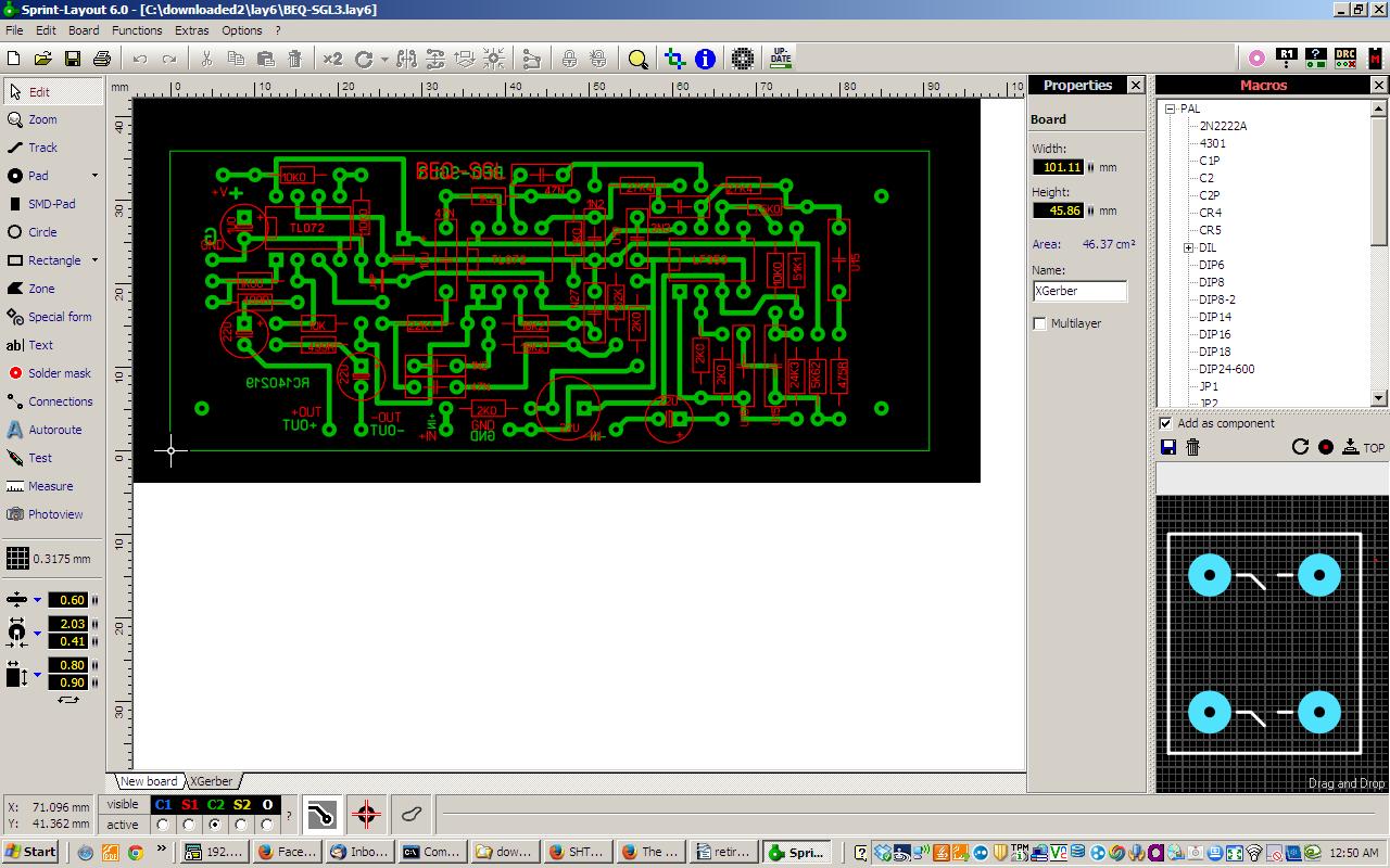
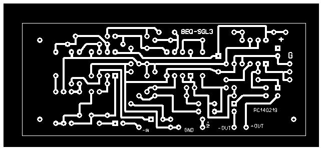
These programs will print to paper at 200% size. As an important suggestion: Place as much text and information as you can to each layer of your board. This helps remind you which side of the board you are exposing. It also helps testing and troubleshooting. See pcb checklist for other helpful tips. The single sided board printout image should look like the artwork below at twice the desired size.
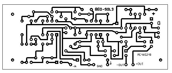
This paper copy should be twice the desired size and is to be reduced down to 50% to obtain the original size.
The image above is what the negative film should look like after it has been
reduced 50% and exposed with the vertical camera. It should be the exact size of
your desired circuitboard. Note: The image shown above is slightly dithered
because it is a graphical representation displayed on this webpage. The lines on
the negative should be sharp and distinctively clear.
Exposing and developing film is similar to black and white paper print enlarging processing. The only difference in the exposing process is you will be reducing the image, not enlarging the image. For this particular camera, with the reduction set to 50%, the lens is set to F22 and the film is exposed for 12 to 15 seconds for the camera pictured above.
Once original artwork is centered on bottom frame, extinguish all but red safety lights. Cut fresh film to proper size. Usually about an inch all around larger. You will notice that one side of the film is lighter than the other. This is the emulsion side. It's actually pinkish in color. Open vacuum frame and start the vacuum pump. Center the film emulsion (lighter) side up on the frame. It should stick on frame tightly. Close vacuum frame and start timer. The exposure lights will illuminate for the preset time. Once the light extinguishes open vacuum frame, turn vacuum off and remove film for developing.
|
Definition of emulsion: All photographic film has a coating of emulsion on one side. This can be observed by holding the developed film at an angle to a source of light. One side will look smooth and glossy. This is the non-emulsion side. The other side will have a matte look and the black portion of the emulsion will have a flat dull appearance. This is the soft emulsion. This side should be the side that is in contact with the sensitized copper clad board. It is important that your exposure should be such that when the emulsion is toward the board, the image, the clear portion, will be the same as the desired copper tracks on the board. If you desire to make the bottom side of the board, you mirror image your printing. Printing the top side you needn't mirror image the printing. In other words the top and bottom negative should look like the desired results of the etched circuitboard. |
The film developing process is almost identical to paper processing. Kodalith or Litho developer is mixed and placed in first tray. A stop bath or plain water is in second tray. Fixer, which is universal for prints and film is used in third tray. A fourth tray or tub in sink is used to wash finished film. The film can be squeegeed and/or just hung to dry.
A red safety light is used to view and handle film during all the processes. I use solid red Christmas lights in about three places in the processing booth.
As you develop the board start with the emulsion (or lighter pink) side up. Agitate the film in all following steps. You should see the image appear after about 15 seconds or so. Weaker solution may take a little longer. Once the image looks pretty defined, turn the film over and observe the image. Once the contrast is well defined, a solid black and solid white, you can take your tongs and hold it up to the red light. You should not see the light bulb in the black portion. If you do, continue to develop until it is totally opaque. If you can still see the red light through the black portion you may have to discard the film and try again. Increase the exposure time by about 5 second increments, or try a fresh batch or stronger developer solution.
Once satisfied with the developing, wash in stop bath for a few seconds then dip in fixer. Leave in fixer until the white or cloudy portion turns perfectly clear. Then leave in about 30 or more seconds longer. The longer the better. It will harden the emulsion even more.
If you were brought to this page via a search engine make sure you study the top page for the actual procedure using negative films in making printed circuit boards.
Below are some sample links to film and chemicals:
Link to 8X10 film from Freestyle Link to developer from Freestyle Link to fixer from Freestyle
Link to 5X7 film from B&H Link to developer from B&H Link to fixer from B&H
Note: This web page is being updated at least weekly if not daily as I get pictures and procedures documented.
Text and pictures Copyright © 2014 by Rick C.
Kodalith and KPR are registered trademarks of The Kodak Corp.
This site has been providing free information for over ten years. We ask for no monetary remuneration. However the cost of keeping this domain and server running has increased substantially. If you are so inclined, you can make a donation no matter how small to keep this site always available. You can click on the Paypal button to donate. You don't need a Paypal account to contribute. Thanks for your support.