The purpose of this web page is to provide information on how to test, troubleshoot, modify or create a guitar effects pedal. You will learn how typical pedals work and even how to build your own.
Effects pedals come in all sizes and shapes. They perform the task of altering the waveform of the incoming signal from the guitar and providing enough drive to reach the guitar amp or another pedal. Pedals can be chained together so you can insert the desired effects by just stepping on a footswitch.
Most pedal connections follow a certain pattern so they all interface basically the same:
1) The input is usually on the right side and the output is on the left. Some have
jacks on the back.
2) Power is derived from either an internal nine volt battery or the coaxial
power connector on the back. The power connector is normally center pin negative,
and outside shell positive. Plugging in an external power plug disconnects the
internal nine volt battery.
3) The pedal requires a standard mono 1/4 inch (tip-sleeve 2 circuit) plug from
an instrument cable
inserted into the input to turn
the unit on. The input plug removed, prevents a pedal that's turned on from discharging the battery.
4)When the effects pedal is turned off, the audio flows from the input
to the output thus bypassing the pedal. There are however differences on how
this occurs and it will be explained in the On/Bypass section.
Effects pedals can do various things. Primarily there are distortion/overdrive/fuzz, tremolo, delay/echo, equalizer, modeling, guitar tuners, noise gates, faders, wah-wah, and some specialized types.
With the exception of the effects stage much of the circuitry is the same from pedal to pedal. Note: The circuits contained on this page are not just theoretical schematics. If you built this pedal exactly like the schematics, it will really work!
Almost every electric guitar player has at least one type of distortion pedal. Distortion is accomplished by diode semiconductors in the feedback section of the effects stage. Different types of diodes, silicon, Germanium, Schottky, MOSFET transistors, even LED's, in different series or parallel combinations all give a unique sound that most players are looking for.
Before going any further it is assumed you know a good bit of audio electronics or are learning it. If you are not sure how to read the schematics and understand the nomenclature (parts values), I would recommend you reading the Component Identification page first. Also it would help if you studied the Basic Op-amp Design tutorial page that will give you more information on how they work. I will simplify an explanation on how to test and troubleshoot op-amp devices too.
Over 90% of all pedals have the same power supply, input, bypass, and output stages. The only thing different is the effects section. The following will explain each circuit and how it functions.
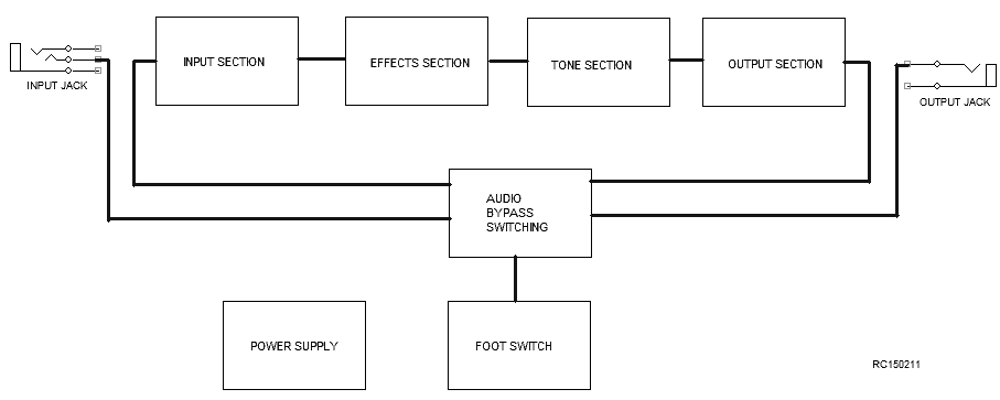
Block diagram (of a typical pedal)
The guitar signal enters the input section on the left. After being enabled by the Audio/Bypass switch, the signal gets modified in the Effects Section. There is sometimes a tone control to boost or cut the higher frequencies. The signal then goes to the output stage that drives the guitar amplifier or another pedal. The footswitch and logic controls the audio bypass circuit.
Input stage
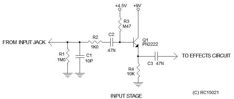
The input section is technically called an emitter follower, driver, or impedance converter. Its purpose is to take the high impedance input coming from the guitar or previous stage and lowers the impedance to around 10,000 ohms to drive the next section. This being the effects.
Technical Details: As you can see, C2 and C3 isolate the DC around the Q1 transistor. Q1 collector is tied to +9 volts. Q1's emitter is tied to ground through R4, a 10K resistor. The base is biased to +4.5 volts through R3 to turn Q1 partially on. This puts about +4.3 volts on the emitter. This circuit is typically called an "Emitter Follower". Its primary purpose is to take a signal into the high impedance input and convert to a low impedance drive of 10K ohms. In an emitter follower there is no gain. Actually there is a slight loss, typically about 10% of the signal but for practical purposes this is insignificant. So a 1.00 volt AC signal on the input will provide about a 0.80 volt signal on the output.
In troubleshooting this circuit it is not necessary to measure the voltage from the base to ground. The voltage on the emitter should give you a clue if this stage is working. It should be somewhere between 2 volts and 5 volts but averaging around 4 volts or half the power supply voltage. This DC voltage is not that critical as long as the audio driving the circuit doesn't exceed the peaks of the waveform. If you do measure the voltage between the emitter and base it should be around 0.7 volts base more positive. Assuming all the capacitors and resistors are good, if the emitter is sitting at around 9 volts or zero volts, the transistor (Q1) is defective.
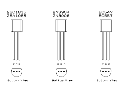
For most stages like this almost any silicon NPN bipolar transistor will work. A 2N2222, 2N3904, 2N4401, PN2222, C1815, etc. If designing your own audio circuit make sure the pinout (base, collector and emitter leads) is correct since they are different depending on part number. This can lead to a lot of confusion if not wired right. See Figure 5 near bottom of this page. R1 keeps any leakage from C2 from building up. C1 takes any unwanted high frequencies out. R2 and C2 roll off frequencies below 800 hertz. C3 blocks any DC from getting to the next stage.
Effects stage - This section is unique for all pedals. The distortion circuit shown below is typical of most distortion pedals
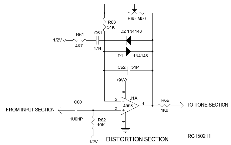
In this example the effects will be a distortion or overdrive circuit. The signal coming from the input section is heavily clipped by the feedback diodes D1 and D2 to provide the fuzzy sound desired. There may be a gain control, drive or boost control and/or a diode selection switch to give that unique sound. Some pedals have a series of diodes in either direction with a rotary switch to select that unique sound. On my second page I will show more on the diode bank.
Tone Stage
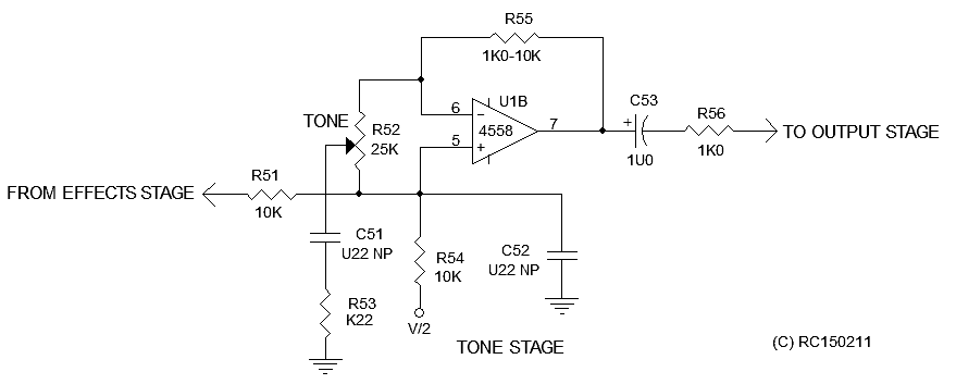
This section usually involves an operational amplifier being controlled by a tone control R52. It typically boosts or cuts the high frequencies. More sophisticated tone controls will boost the highs and cut the lows and vice versa.
Technical Details: This section is pretty much straight forward. The gain determined by R55. This value may have to be adjusted depending on the level coming from the effects section. It should be set so when you punch in and out the effects the overall level should be about the same. The higher the value the more the gain. The tone control provides either a low frequency boost/cut or high frequency boost/cut by providing a variable capacitance from the (+) input to the (-) input. As with all opamps operating in the linear mode you should have +4.5 volts DC on both inputs and the output. If not, there is a problem in this stage.
Output Stage
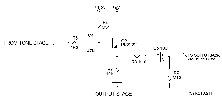
The output section looks similar to the input stage. It takes the high level, high impedance signal from the preceding stage and provides a larger drive level at a lower impedance to the guitar amplifier or next pedal. What is not shown is just before the R5 input there should be a 10K to 100K volume pot. The wiper tied to R5, Low side tied to ground or 4.5 volt reference and the high side to the previous stage.
Technical Details: This is very similar to the input section with the addition of R8 and R9. R8 provides some short circuit protection so damage to Q2 will not occur. C5 blocks any DC from the emitter follower stage getting to the output. R9 bleeds of any residual build up of voltage due to any slight leakage across C5. This will prevent any damaging and annoying DC "pop" if a plug is inserted to the output jack. As with the input stage, the emitter should be around half the 9 volt power supply but could be from 2 volts to 6 volts DC.
All pedals have a way of inserting the effects and bypassing the effects when unwanted. The performer just has to depress the pedal on top of the unit to insert the effects or bypass them. There are two ways this is accomplished. The most popular way, the active bypass, is a large square pad on the top front of the pedal. Stepping on it will turn the effects on or off. It usually makes no mechanical click when depressed with your foot. This method is an electronic flip-flop circuit with FET (field effect transistor) transistors switching the signal in and out. When out (bypassed), it usually sends the same signal from the input jack right to the output without marring the sound....for the most part. A lot has been written about the quality of this method. It is said it doesn't faithfully pass the original sound through the pedal.
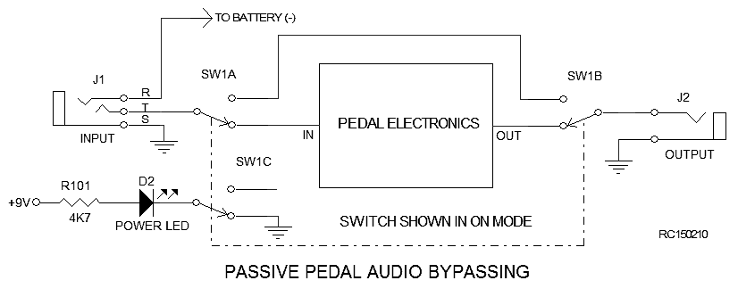
The circuit below shows a passive bypass hard switch consisting of a round chrome button. Stepping on it brings on an audible mechanical click as it switches in and out. These faithfully route the exact signal from the input to the output even when the power is turned off and thus not marring the sound.
On/Bypass Passive Switching
This is how a passive true bypass is accomplished.
On/Bypass Active Switching
Active FET switching is common in most pedals although not as desirable as passive switching. Why? Because the active switching may not faithfully reproduce the same output as the input. To some this may not matter but for others that are serious about keeping their sound pure will notice. Having three or more active pedals in series and you may loose some quality.
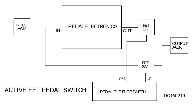
There is a transistor flip flop circuit that changes state when the pedal button is depressed. A flip flop is a two-state circuit that will change its logic output each time the pedal switch is depressed. The logic output turns one FET switch on at a time and not both. As you can see by the above block diagram the FET switches will pick up the audio from either the raw input or the effects output.
The circuit below is exactly how the audio is switched.
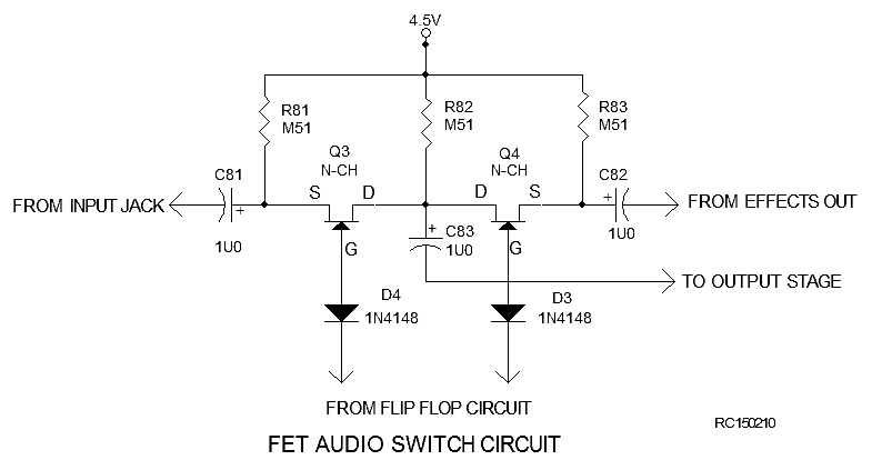
The theory behind the FET is as follows: The input (drain) and output (source) are usually biased at V/2 or half the 9 volt supply. When the gate is biased (turned) on, the FET conducts and acts like an audio switch. The drain and source can be swapped since the audio can flow either way. A typical N-CH Junction FET is a 2N5457, 2N5458, 2SK30ATM. Observe the proper pinouts on these devices.
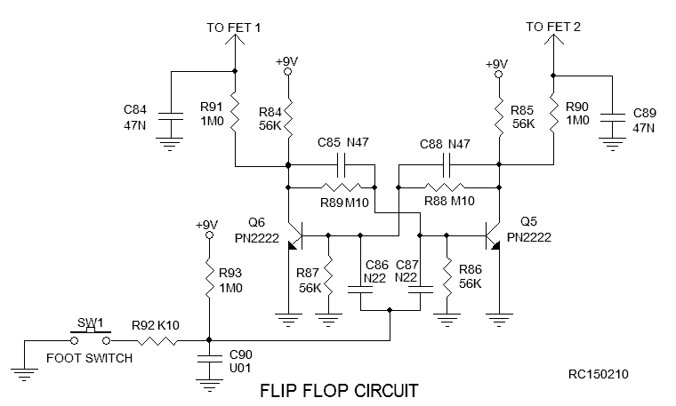
This circuit above is a bi-stable flip flop. Upon receiving a pulse from the foot switch the flip flop changes state. The output from the flip flop drives both FETs turning only one or the other on.
Power Supply
Most pedals get their power from a 9 volt supply. This is either a 9 volt battery, or an external "wall wart" or multi tap power unit that provides power to a number of pedals at the same time.
Usually on the rear of the pedal is a round recessed coaxial jack. Marked in the back of the pedal is the proper polarity required for the pedal.


As you can see most pedals have a "center negative" pin. I know of only the first model of the JangleBox that has the power input reversed. I think later models corrected this. Make sure you use the proper power cable otherwise damage to the pedal may occur. Typically there is a protect diode in the pedal to prevent a wrong polarity power supply from damaging the pedal but sometimes the diode falls short of protection depending on the diode.
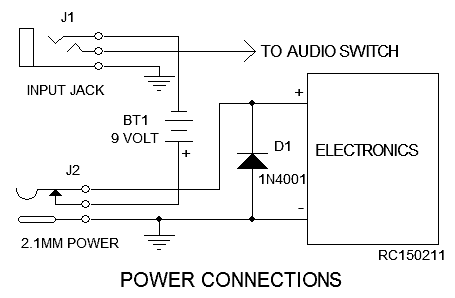
With no external power connected, the circuit is energized when a two circuit plug (standard instrument cable) is inserted into the input jack. The sleeve or ground on the plug shorts the ring contact to ground and connects the battery minus to ground energizing the electronics. If an external power plug is inserted, the battery is disconnected and power is routed from the external supply to the electronics. A protect diode D1 should be installed in this part of the circuit. This will protect the electronics in case an external supply of reversed voltage or and AC supply is accidentally inserted.
| Note: If you have a plug inserted into the input jack and you are not using an external power supply, the electronics is turned on and the battery is discharging slowly even though it is in the off or bypass mode. After about a week the battery will be dead. |
|
Caution: Be aware that many pedal schematics of power circuits drawn and posted to the internet are drawn wrong and cannot possibly work like the factory pedals. |
Study exactly how this circuit works and you will have a trouble free design.
Power Supply Biasing
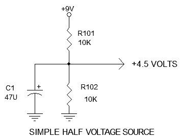
For most pedal applications the voltage divider circuit above is all that is necessary to produce a half supply voltage and can be found in almost all effects pedals. A half voltage is required when you power an opamp from a single 9 volt power supply. It works by placing two identical value resistors in series across the power supply (9 volts) and ground. The result is half the supply voltage, +4.5 volts, where the two resistors meet. There is a filter capacitor at the half way point to filter out any variations in voltage and provide a low impedance power source for circuit biasing.
R101 and R102 can be of any value between 4K7 ohms and 15K ohms as long as they are both the same but the norm is 10K because they are so common and the more of the same values used in a project the cheaper it can be built. Anything less than 4K7 ohms and it will provide too much draw from the battery. Any value higher and you could have a stability problem as the voltage may fluctuate. This source should be as close to 4.5 volts and as stable as possible.
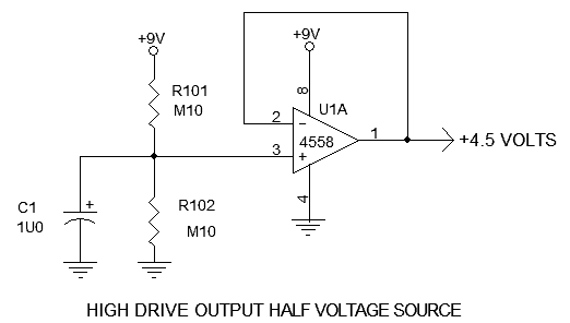
The circuit above is a "follower" circuit. It uses an op-amp to provide a high amount of drive especially if there is more of a demand for the 4.5 volts in the pedal. Because the input impedance on the (+) input is so high, almost any higher value resistors can be used for the voltage divider R101 and R102. In this case M10 (100k) values and a smaller filter capacitor is used.
Why is 4.5 volts important? Operational amplifier integrated circuits usually operate from a plus (+) and minus (-) power supply from ground. Since most pedals operate only from a single nine volt battery, the (-) pin of the opamp is tied to ground and the (+) is tied to +9 volts. The +4.5 volts biases the inputs of the opamp half way to 9 volts to "cheat" the opamp into thinking it has the + and - volts to function in its linear region.
|
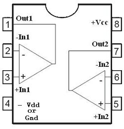
Important troubleshooting hint!!! Since operational amplifiers such as the 4558 are biased with 4.5 volts (or some voltage close) in this type of circuit, ALL input and output pins will idle at the same voltage. If not, the opamp is not functioning. If you suspect a bad opamp, take a voltmeter and measure the voltage on all four inputs and two outputs (if both sections of the chip are used). All the pins should be idling at the same voltage. If not, either the opamp is bad or some other external component is defective. Either open or shorted. |
|
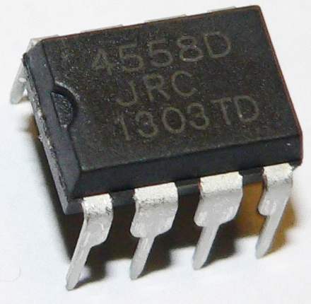
The 4558 Operational Amplifier The 4558 opamp is probably the most popular audio opamp in most pedals. Particularly the JRC4558 device. All 4558 devices are the same from manufacturer to manufacturer but some claim the JRC4558 has a more "desired" sound. I have not witnessed that but will go along with this anecdote for the time being. The 4558 consists of two independent operational amplifiers with common power pins. Pin 8 is (+) power and pin 4 is (-) power. Other dual opamps can and will work in this type of pedal. A MC1458, TL072, TL082, LM318, LF356, CA3140, etc.
The nice thing about these amplifier chips is that they can be programmed to provide the desired gain and don't require any external frequency compensation. They have a very high input impedance and a very low output impedance. Meaning they will not load a preceding stage and can provide a lot of drive for the next stage. If you are confused or want to learn more about opamps, study my Basic Opamp Design page. |
|
|
Figure 5
Audio specifications surrounding the guitar, pedal and amp stages:
The average level from a guitar with the guitar volume turned on full is about 50 millivolts or 0.05 volts. Peak levels are around 100 millivolts or 0.10 volts.
In order to test, analyze, and demonstrate how all of the above circuits work I built a live demo unit as shown below.
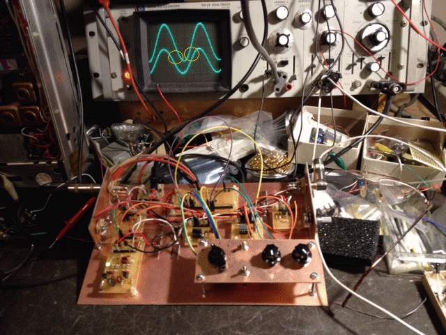
This allowed me to test different modules by just plugging and unplugging each circuit as needed. As you can barely see on the scope there is a slight phase shift from the input to the output of the input stage. You can just see the spacing of the two waveforms in the two yellow circles. To be in phase the waveforms would be exactly on top of each other. First I thought there was something wrong but then looking at the schematic I remembered there was a filter, R2 and C2 that rolls of the low frequencies which appears as a shift in phase. The top waveform is a 250 millivolt swing on a 50 mv/div display. You can see on the lower waveform that there is only a 200 millivolt swing demonstrating the loss in the emitter follower stage.
If you would like to build a working prototype/demo unit for experimentation, click here for the details.
If you are planning on building a pedal from scratch or need repair parts check out my link to Pedal Parts.
Questions and comments can be directed to Rick C.
All pictures and text are Copyright ©2015 by Rick C. You may freely copy and quote this page as long as nothing is modified and credit is given to the website Neatcircuits.com. I would prefer you dropping me an email letting me know how you are using this info.